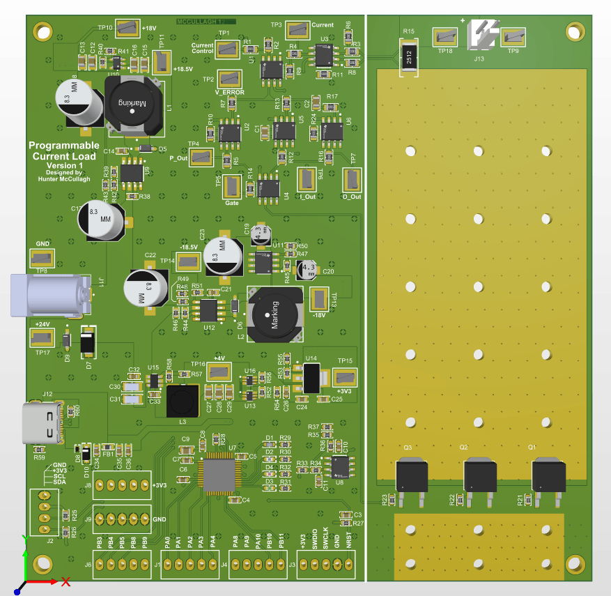
3D model of Programmable Current Load
Background
The purpose of this project is to create an electronics evaluation tool to see how circuits function when a current drain is applied.
The inspiration for this project was a need to deplete the battery of its charge to monitor the systems performance.
The idea then further developed into creating a tool that can act as an ideal current load similar to what might be seen in a SPICE model. This can be useful for when bringing designs out of SPICE simulation and onto the benchtop for direct comparison.
Electrical Design
The focal point of the design revolves around the analog control loop, which measures current going through the current sense resistor, compares the current with the bias voltage set by the microcontroller, and then employs a tuned PID output to the gate pins of some MOSFETs to achieve the correct current draw.
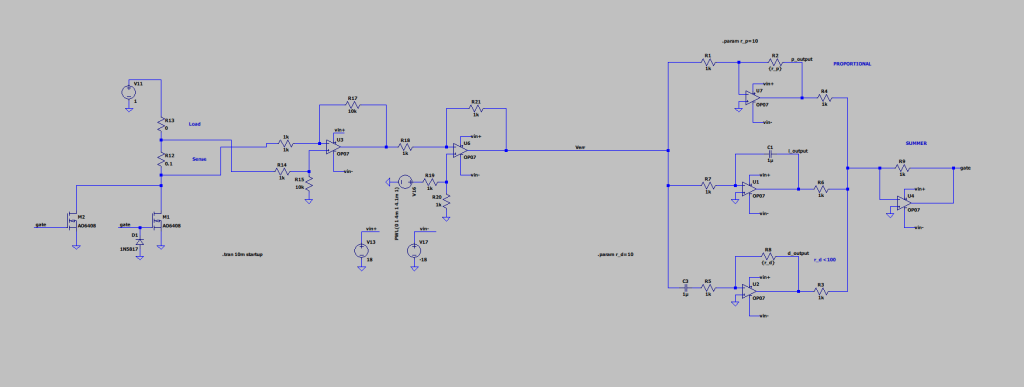
Current Control Loop
The design uses OP07 op amps that are powered with +-18V power rails.
In terms of power to the system, a 24V wall wart is used to provide power to the system and then a series of buck converters and LDOs are used to generate +-18V and +3.3V.
An additional feature is that the USB-C input voltage is passed through a series of ideal diodes with the 24V wall wart so that the STM32 microcontroller can still be powered and programmed even when the wall wart isn’t used.
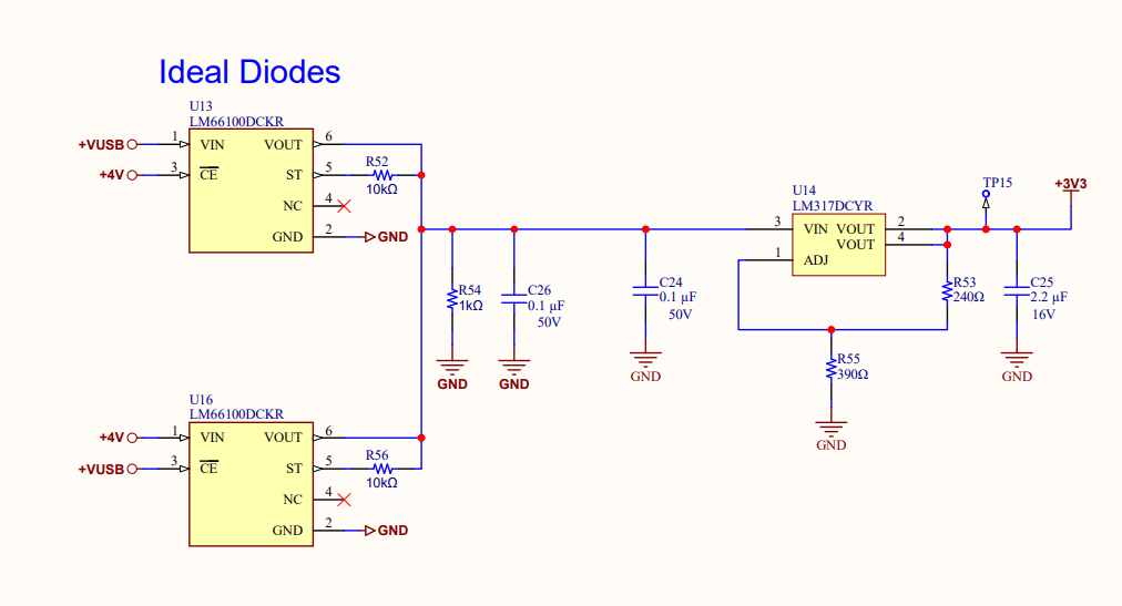
Ideal Diode Configuration
Additonal GPIO have been routed so that additional features can be added to the circuit board, such as an OLED, a dial to control current, and switches.
Firmware
Circuit Board is ordered from JLCPCB, firmware development will begin when I receive boards.
Validation
Waiting on PCBs to come in.

